
Author Affiliations
Abstract
1 Key Laboratory for Information Science of Electromagnetic Waves (MoE), Department of Communication Science and Engineering, Fudan University, Shanghai 200433, China
2 National Institute of LED on Silicon Substrate, Nanchang University, Nanchang 330096, China
In recent studies, visible light communication (VLC) has been predicted to be a prospective technique in the future 6G communication systems. To suit the trend of exponentially growing connectivity, researchers have intensively studied techniques that enable multiple access (MA) in VLC systems, such as the MIMO system based on LED devices to support potential applications in the Internet of Things (IoT) or edge computing in the next-generation access network. However, their transmission rate is limited due to the intrinsic bandwidth of LED. Unfortunately, the majority of visible light laser communication (VLLC) research with beyond 10 Gb/s data rates concentrates on point-to-point links, or using discrete photodetector (PD) devices instead of an integrated array PD. In this paper, we demonstrated an integrated PD array device fabricated with a Si-substrated GaN/InGaN multiple-quantum-well (MQW) structure, which has a array of micro-PD units with a common cathode and anode. This single-integrated array successfully provides access for two different transmitters simultaneously in the experiment, implementing a MIMO-VLLC link at 405 nm. The highest data rate achieved is 13.2 Gb/s, and the corresponding net data rate (NDR) achieved is 12.27 Gb/s after deducing the FEC overhead, using 2.2 GHz bandwidth and superposed PAM signals. Furthermore, we assess the Huffman-coded coding scheme, which brings a fine-grain adjustment in access capacity and enhances the overall data throughput when the user signal power varies drastically due to distance, weather, or other challenges in the channel condition. As far as we know, this is the first demonstration of multiple visible light laser source access based on a single integrated GaN/InGaN receiver module.
Photonics Research
2024, 12(4): 793

Author Affiliations
Abstract
Although the 5G wireless network has made significant advances, it is not enough to accommodate the rapidly rising requirement for broader bandwidth in post-5G and 6G eras. As a result, emerging technologies in higher frequencies including visible light communication (VLC), are becoming a hot topic. In particular, LED-based VLC is foreseen as a key enabler for achieving data rates at the Tb/s level in indoor scenarios using multi-color LED arrays with wavelength division multiplexing (WDM) technology. This paper proposes an optimized multi-color LED array chip for high-speed VLC systems. Its long-wavelength GaN-based LED units are remarkably enhanced by V-pit structure in their efficiency, especially in the “yellow gap” region, and it achieves significant improvement in data rate compared with earlier research. This work investigates the V-pit structure and tries to provide insight by introducing a new equivalent circuit model, which provides an explanation of the simulation and experiment results. In the final test using a laboratory communication system, the data rates of eight channels from short to long wavelength are 3.91 Gb/s, 3.77 Gb/s, 3.67 Gb/s, 4.40 Gb/s, 3.78 Gb/s, 3.18 Gb/s, 4.31 Gb/s, and 4.35 Gb/s (31.38 Gb/s in total), with advanced digital signal processing (DSP) techniques including digital equalization technique and bit-power loading discrete multitone (DMT) modulation format.
GaN-based LED LED array VLC V-pit sidewall quantum well high-frequency response Opto-Electronic Science
2023, 2(5): 230005

Author Affiliations
Abstract
1 Key Laboratory for Information Science of Electromagnetic Waves (MoE), Fudan University, Shanghai 200433, China
2 Shanghai Engineering Research Center of Low-Earth-Orbit Satellite Communication and Applications, Shanghai 200433, China
3 Shanghai Collaborative Innovation Center of Low-Earth-Orbit Satellite Communication Technology, Shanghai 200433, China
4 National Institute of LED on Silicon Substrate, Nanchang University, Nanchang 330096, China
5 Peng Cheng Laboratory, Shenzhen 518055, China
6 e-mail:
7 e-mail:
8 e-mail:
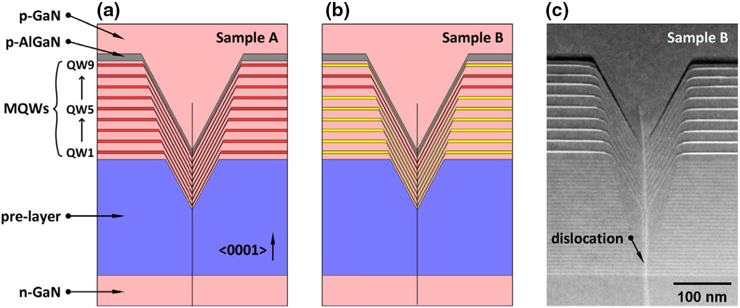
Visible light communication (VLC) has emerged as a promising communication method in 6G. However, the development of receiving devices is much slower than that of transmitting devices, limited by materials, structures, and fabrication. In this paper, we propose and fabricate an InGaN/GaN multiple-quantum-well-based vertical-structure micro-LED-based photodetector (μPD) on a Si substrate. A comprehensive comparison of the photoelectrical performance and communication performance of three sizes of μPDs, 10, 50, and 100 μm, is presented. The peak responsivity of all three μPDs is achieved at 400 nm, while the passband full-widths at half maxima are 87, 72, and 78 nm for 10, 50, and 100 μm μPDs, respectively. The cutoff bandwidth is up to 822 MHz for 50 μm μPD. A data rate of 10.14 Gbps is experimentally demonstrated by bit and power loading discrete multitone modulation and the proposed digital pre-equalizer algorithm over 1 m free space utilizing the self-designed 50 μm μPD array as a receiver and a 450 nm laser diode as a transmitter. This is the first time a more than 10 Gbps VLC system has been achieved utilizing a GaN-based micro-PD, to the best of our knowledge. The investigation fully demonstrates the superiority of Si substrates and vertical structures in InGaN/GaN μPDs and shows its great potential for high-speed VLC links beyond 10 Gbps.
Photonics Research
2022, 10(10): 2394
Author Affiliations
Abstract
1 Key Laboratory for Information Science of Electromagnetic Waves (MoE), Fudan University, Shanghai 200433, People’s Republic of China
2 National Institute of LED on Silicon Substrate, Nanchang University, Nanchang 330096, People’s Republic of China
3 State Key Laboratory of Precision Spectroscopy, East China Normal University, Shanghai 200241, People’s Republic of China
4 State Key Laboratory of Optical Communication Technologies and Networks, China Information Communication Technologies Group Corporation, Wuhan 430000, People’s Republic of China
5 Peng Cheng Laboratory, Shenzhen, 518055, China
High-speed visible light communication (VLC), as a cutting-edge supplementary solution in 6G to traditional radio-frequency communication, is expected to address the tension between continuously increased demand of capacity and currently limited supply of radio-frequency spectrum resource. The main driver behind the high-speed VLC is the presence of light emitting diode (LED) which not only offers energy-efficient lighting, but also provides a cost-efficient alternative to the VLC transmitter with superior modulation potential. Particularly, the InGaN/GaN LED grown on Si substrate is a promising VLC transmitter to simultaneously realize effective communication and illumination by virtue of beyond 10-Gbps communication capacity and Watt-level output optical power. In previous parameter optimization of Si-substrate LED, the superlattice interlayer (SL), especially its period number, is reported to be the key factor to improve the lighting performance by enhancing the wall-plug efficiency, but few efforts were made to investigate the influence of SLs on VLC performance. Therefore, to optimize the VLC performance of Si-substrate LEDs, we for the first time investigated the impact of the SL period number on VLC system through experiments and theoretical derivation. The results show that more SL period number is related to higher signal-to-noise ratio (SNR) via improving the wall-plug efficiency. In addition, by using Levin-Campello bit and power loading technology, we achieved a record-breaking data rate of 3.37 Gbps over 1.2-m free-space VLC link under given optimal SL period number, which, to the best of our knowledge, is the highest data rate for a Si-substrate LED-based VLC system.

Author Affiliations
Abstract
1 Key Laboratory for Information Science of Electromagnetic Waves (MoE), Department of Communication Science and Engineering, Fudan University, Shanghai 200433, China
2 National Institute of LED on Silicon Substrate, Nanchang University, Nanchang 330096, China
3 State Key Laboratory of Optical Communication Technologies and Networks, China Information Communication Technologies Group Corporation, Wuhan 430074, China
High-speed visible light communication (VLC) using light-emitting diodes (LEDs) is a potential complementary technology for beyond-5G wireless communication networks. The speed of VLC systems significantly depends on the quality of LEDs, and thus various novel LEDs with enhanced VLC performance increasingly emerge. Among them, InGaN/GaN-based LEDs on a Si-substrate are a promising LED transmitter that has enabled VLC data rates beyond 10 Gbps. The optimization on the period number of superlattice interlayer (SL), which is a stress-relief epitaxial layer in a Si-substrate LED, has been demonstrated to be an effective method to improve Si-substrate LED’s luminescence properties. However, this method to improve LED’s VLC properties is barely investigated. Hence, we for the first time experimentally studied the impact of SL period number on VLC performance. Accordingly, we designed and fabricated an integrated 4 × 4 multichromatic Si-substrate wavelength-division-multiplexing LED array chip with optimal SL period number. This chip allows up to 24.25 Gbps/1.2 m VLC transmission using eight wavelengths, which is the highest VLC data rate for an InGaN/GaN LED-based VLC system to the best of our knowledge. Additionally, a record-breaking data rate of 2.02 Gbps over a 20-m VLC link is achieved using a blue Si-substrate LED with the optimal SL period number. These results validate the effectiveness of Si-substrate LEDs for both high-speed and long-distance VLC and pave the way for Si-substrate LED design specially for high-speed VLC applications.
Photonics Research
2021, 9(8): 08001581
1 宁波大学 光电子功能材料重点实验室, 宁波 315211
2 大连海事大学 物理系, 大连 116026
采用改进的坩埚下降法成功生长了Ce 3+/Yb 3+离子双掺杂LiLuF4单晶, Ce 3+的初始离子掺杂浓度为0.1mol%, Yb 3+离子浓度从0变化到2.0mol%。在波长291 nm激发时观察到Yb 3+在1020 nm( 2F5/2→ 2F7/2)附近的强近红外发射以及Ce 3+在300~350 nm(5d→4f)的紫外发射。通过吸收光谱、荧光光谱研究了Yb 3+离子掺杂浓度对Ce 3+/Yb 3+共掺杂LiLuF4单晶光谱性质的影响及Ce 3+到Yb 3+离子的能量转移机理。通过变温光谱的研究发现, 当环境温度从298 K增加到443 K时, 其荧光发射强度不断降低。Ce 3+/Yb 3+共掺杂LiLuF4单晶发光波长主要位于紫外和近红外, 这种独特的发光属性可望用于防伪技术和公共安全事务中。
Ce
3+/Yb
3+ 紫外和近红外发射 LiLuF4单晶 能量转移 Ce
3+ and Yb
3+ ultraviolet and infrared emissions LiLuF4 single crystal energy transfer
1 南昌大学,国家硅基LED工程技术研究中心,南昌 330096
2 南昌硅基半导体科技有限公司,南昌 330096
3 江西金黄光智慧照明有限责任公司,南昌 330031
可见光发光二极管(LED)范围内,因“黄光鸿沟”这一世界难题的存在,照明用白光LED主要通过蓝光LED芯片激发黄色荧光粉来实现。然而,由于荧光粉的光光转换效率在自身发热所产生的高温环境中易出现衰退的现象,导致荧光型白光LED在使用过程中容易出现光衰、色温飘移等问题。本团队在高光效InGaN黄光LED取得突破的基础上,利用高光效的红、黄光LED合成了一种新型的低色温LED光源器件,其具有无荧光粉、无蓝光的技术特点,本文称之为“硅基金黄光LED”。当LED芯片工作电流密度为20 A/cm2时,硅基金黄光LED器件的色温为2 170 K,光效为156 lm/W,显色指数Ra为77,当LED芯片工作电流密度为1 A/cm2时,光效可达217 lm/W。本文报道了这一新型LED器件的光效和色温随电流和环境温度的变化趋势,同时对该器件的空间光谱分布进行了优化研究。此外,开展了该器件的高温、高温高湿、冷热冲击等可靠性型式试验,验证了硅基金黄光LED器件具有高可靠性的特点。最后,本文介绍了硅基金黄光LED器件在道路照明、隧道照明等领域的示范应用,以及在母婴灯等家居照明领域的推广应用。
硅基金黄光LED 多基色LED 无荧光粉 无蓝光 可靠性 照明应用 siliconbased golden light LED color mixed LED no phosphor no blue light reliability lighting application
Author Affiliations
Abstract
National Institute of LED on Silicon Substrate, Nanchang University, Nanchang 330096, China
Indium gallium nitride (InGaN)-based light-emitting diodes (LEDs) are considered a promising candidate for red-green-blue (RGB) micro displays. Currently, the blue and green LEDs are efficient, while the red ones are inefficient for such applications. This paper reports our work of creating efficient InGaN-based orange and red LEDs on silicon(111) substrates at low current density. Based on the structure of InGaN yellow LEDs, by simply reducing the growth temperature of all the yellow quantum wells (QWs), we obtained 599 nm orange LEDs with peak wall-plug efficiency (WPE) of 18.1% at . An optimized QW structure was proposed that changed two of the nine yellow QWs to orange ones. Compared with the sample containing nine orange QWs, the sample with two orange QWs and seven yellow QWs showed similar emission spectra but a much higher peak WPE up to 24.0% at with a wavelength of 608 nm. The improvement of peak WPE can be attributed to the improved QW quality and the reduced active recombination volume. Subsequently, a series of efficient InGaN-based orange and red LEDs was demonstrated. With further development, the InGaN-based red LEDs are believed to be attainable and can be used in micro LED displays.
Photonics Research
2020, 8(11): 11001671
Author Affiliations
Abstract
1 National Institute of LED on Silicon Substrate, Nanchang University, Nanchang 330096, China
2 Nanchang Yellow Green Lighting Company Limited, Nanchang 330096, China
3 e-mail: liujunlin@ncu.edu.cn
Realization of efficient yellow-light-emitting diodes (LEDs) has always been a challenge in solid-state lighting. Great effort has been made, but only slight advancements have occurred in the past few decades. After comprehensive work on InGaN-based yellow LEDs on Si substrate, we successfully made a breakthrough and pushed the wall-plug efficiency of 565-nm-yellow LEDs to 24.3% at 20 A/cm2 and 33.7% at 3 A/cm2. The success of yellow LEDs can be credited to the improved material quality and reduced compressive strain of InGaN quantum wells by a prestrained layer and substrate, as well as enhanced hole injection by a 3D pn junction with V-pits.
Photonics Research
2019, 7(2): 02000144
太原理工大学 建筑与土木工程学院, 山西 太原 030024
焊接空心球网架结构被广泛使用在带悬挂吊车的工业厂房中。悬挂吊车带来的往复交变荷载会造成网架焊接节点的疲劳破坏。在焊接空心球节点的疲劳试验过程中, 借助红外热像仪记录试件表面的温度, 得到了试件表面的温升分布, 温升高区位于钢管与焊接球的焊接连接球面焊趾处, 此区域对应节点最后的疲劳破坏位置。在疲劳试验过程中, 焊趾处的温升高区位置几乎不变, 当疲劳裂纹穿透球壁厚时, 温升高区的位置发生变化。试验表明: 红外热像仪可以实时记录焊接空心球节点试件在疲劳试验过程中表面的温度, 通过分析温升高区在没有可见裂纹的情况下就可预测疲劳破坏发生的位置, 温升高区位置的变化对应裂纹贯穿球壁时节点试件的疲劳寿命。
焊接空心球节点 疲劳破坏 红外热像法 穿透裂纹 welded hollow spherical joints fatigue failure infrared thermography through-thickness crack 红外与激光工程
2018, 47(8): 0804002


